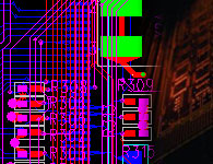
High-speed PCB designs including high-speed digital, analog, mixed-signal (digital/analog), RF, and power supply designs.
High layer-count PCB designs (up to 30 layers) with ultra-high-density layouts.
Impedance-controlled PCB designs with delay matching, stack-up optimization, and material selection.
Wireless LAN PCB designs supporting IEEE 802.11x and IEEE 802.15.4 standards, including fine-pitch BGA (0.4 mm) with up to 1512 pins.
PCB designs with Micro Vias, Blind Vias, Buried Vias, and Backdrill technology.
Motherboards, Single Board Computers (SBCs), High-Speed Serial Backplanes, and Telecom Backplanes.
ASIC Test Boards, Load Boards, Probe Cards, Burn-in Boards, Sockets, and Package Design.
Standards-compliant PCB designs following IPC, UL, MIL, and DO-254 guidelines.
High-speed interconnect designs supporting data rates up to 10 Gbps.
Pre-route and Post-route Signal Integrity Analysis, including IBIS Model Creation.
EMI Analysis and Power Integrity (PI) Analysis.
Signal quality analysis including Crosstalk, Reflections, Timing, Eye Diagram, and Bit Error Rate (BER).
Board-level and System-level Thermal Design, Simulation, Analysis, and Multi-board Thermal Analysis.
Design for Testability (DFT), Design for Manufacturability (DFM), and Design for Serviceability (DFS).
Mechanically and Thermally Constrained PCB Designs.
PCB Deisgn Services
Outsourcing PCB design allows companies to focus on their core strengths whether product strategy, marketing, or system integration while experienced engineers handle complex design work. By leveraging external expertise, businesses can reduce time-to-market, improve design reliability, and optimize manufacturing readiness.